HMDS Bake Plate
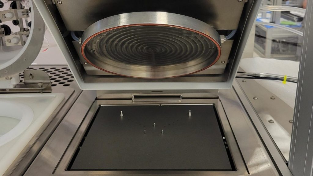
Amplifying Adhesion: HMDS Bake Our client faced persistent issues with photoresist delamination during the photolithography process. To address this, we implemented a solution involving Hexamethyldisilazane (HMDS) priming using the Apogee® 200mm Bake Plate. This enhanced photoresist adhesion, improved yield, reduced defects, and lowered costs, ultimately streamlining project timelines. Additionally, a 75° contact angle was achieved […]
UV Cure Spin Coater
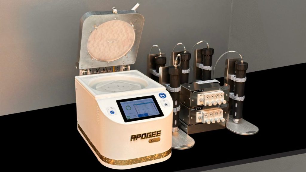
UV Cure Spin Coater A leading nanophotonics and nano-optic security company partnered with Cee® to develop a custom UV cure spin coater. The tool integrates UV curing with spin coating, preventing oxidation and ensuring consistent, high-quality production of nanostructured materials. Introduction In the highly specialized field of nanophotonics and nano-optic features, precision and process control […]
Large Format Spin Coater
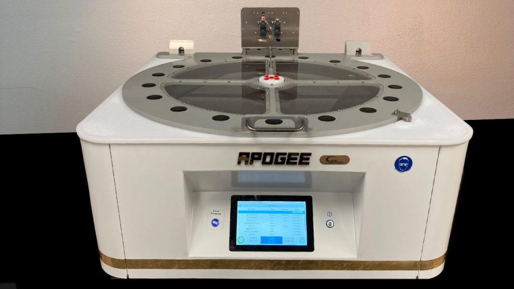
Large Format Spin Coater In the realm of genetic engineering, diagnostic nanomaterials, and high-precision diagnostic equipment, precision and uniformity are paramount. When a leading company in this industry required a specialized spin coater to apply thin, uniform coatings of functionalized nanomaterials onto substrates, they turned to Cee®. This case study highlights the collaboration between Cee® […]
The Art of Manual Dispense
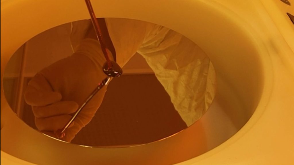
While automated solutions offer convenience and consistency, manual dispense for spin coating remains an invaluable technique, providing precise control and unmatched flexibility. In this article, we’ll discuss the benefits of manual dispensing for spin-coating semiconductor substrates, offering insights, tips, and best practices for this approach. Spin Coating Basics Spin coating is a widely used technique […]
NRTL! What is it good for?
NRTL certification is becoming crucial for semiconductor equipment manufacturers as it ensures compliance with safety standards set by regulatory bodies like OSHA and ANSI. It also facilitates market access, instills customer confidence, provides liability protection, and encourages continuous improvement in safety and quality practices. For custom equipment, additional evaluations may be required. In years to […]
Mini-Spin Coater
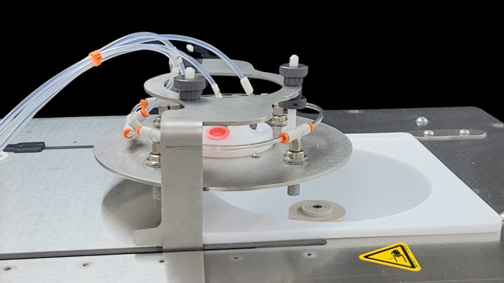
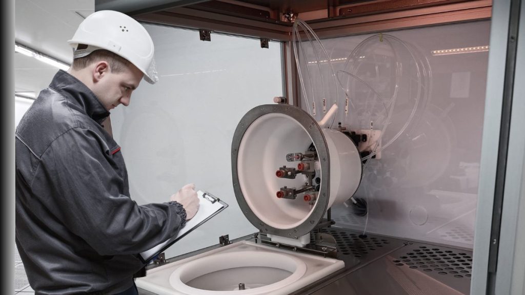
Mini-Spin Coater A photovoltaic research institute required a compact spin coater to integrate with a robotic work cell. Cee® created a custom coater with a 120mm Teflon™ bowl, a mechanized lid, and auto-dispense functionality. This solution met the institute’s high-speed control needs, chemical compatibility, and space constraints. In production, the coater exceeded expectations, delivering safety […]
Beyond the Bond: Semiconductor Debonding Practices
Debonding is a vital step in advanced semiconductor manufacturing and 3D Packaging that involves separation of the device wafer from its carrier. This article includes an overview of a variety of debonding methods, including Laser, Thermal, Chemical, and Mechanical Debonding along with crucial factors for success. The Vital Role of Debonding in Semiconductor Manufacturing Before […]
Bond_Debond
Bond / Debond Bond / Debond Blog Navigation Blog Home Spin Bake Develop Bond_Debond Accessories Bonding_Debonding Bonding and Debonding Indium Phosphide Wafers October 3, 2023 Bonding_Debonding Wafer Bonding Theory August 8, 2023
Bonding and Debonding Indium Phosphide Wafers
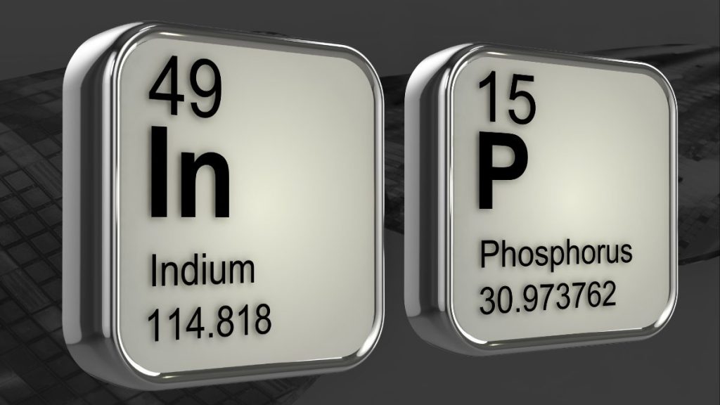
Indium phosphide (InP) wafers present challenges in bonding/debonding due to thermal mismatch, surface damage risks, and material compatibility issues. Cee® provides precision wafer handling tools with customized process controls designed to tackle the challenges presented by InP wafers. Experience reliable wafer handling and fully utilize the exceptional properties of InP for advanced electronics/photonics. Introduction Indium […]