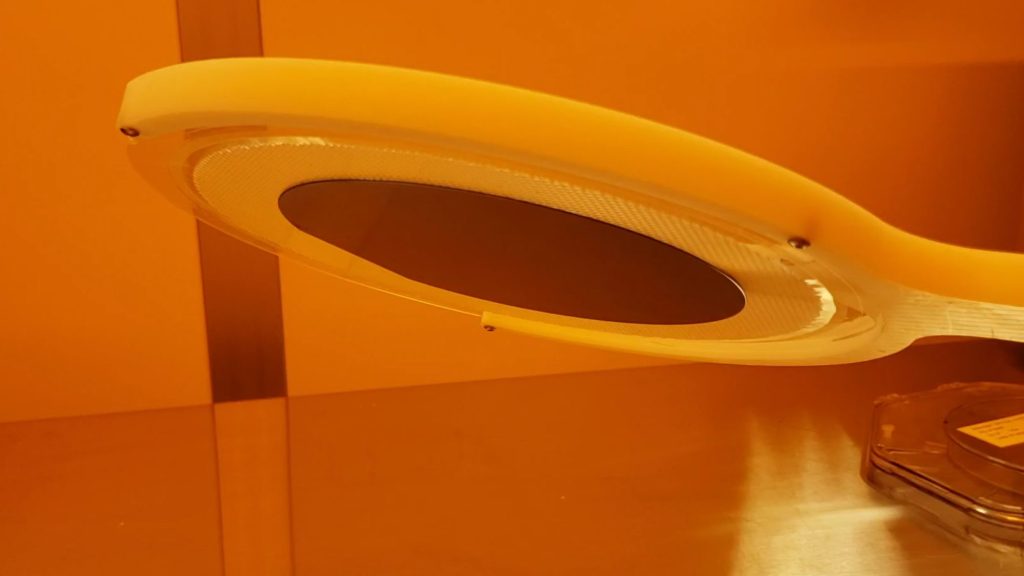
Debonding is a vital step in advanced semiconductor manufacturing and 3D Packaging that involves separation of the device wafer from its carrier. This article includes an overview of a variety of debonding methods, including Laser, Thermal, Chemical, and Mechanical Debonding along with crucial factors for success.
The Vital Role of Debonding in Semiconductor Manufacturing
Before advanced manufacturing processes can take place, semiconductor wafers are temporarily bonded to carrier substrates. This temporary bond provides mechanical stability during processes like thinning, layer deposition, and device integration. Temporary bonding safeguards the delicate semiconductor components from damage, ensuring their integrity throughout the manufacturing process.
Debonding involves carefully detaching the device wafer from its temporary carrier substrate once the desired processes have been completed. This delicate procedure requires precision and finesse, and significantly impacts the quality, performance, and viability of the final device. Through precise debonding practices, manufacturers can fine-tune wafer properties, such as thickness, stress distribution, and material composition thereby optimizing electronic functionality.
Crucial Factors for Successful Debonding
For successful debonding, several factors must be considered:
Adhesive Material Selection: Choosing the appropriate adhesive material is essential. The adhesive’s properties, such as its strength, compatibility with the debonding method, and thermal and material tolerance impact the success of the debonding process.
Process Control and Parameters: Maintaining precise control over process parameters like temperature, pressure, and force is critical. Deviations from optimal conditions can lead to inconsistent or undesirable debonding outcomes.
Surface Preparation: Properly preparing the substrate surface is vital for achieving optimal adhesion and subsequent successful debonding. Adequate cleaning, surface treatment, and roughness can impact the bonding strength and efficiency of the debonding process.
Carrier Design: The design of the temporary carrier substrate affects the ease of debonding. An optimized carrier design can minimize stress concentrations and ensure uniform force distribution during the debonding process. Matching the carrier’s coefficient of thermal expansion to that of the device wafer helps prevent issues like wafer warpage and breakage post-debonding.
Compatibility with Substrate Material: Consider the compatibility of the debonding method with the properties of the substrate material, such as its thermal sensitivity, brittleness, and anisotropic behavior. Certain debonding methods may be better suited for specific materials.
Quality Control and Inspection: Regular monitoring and inspections throughout the debonding process help identify potential issues early on. This practice minimizes waste and ensures consistent, high-quality results.
Post-Debonding Processes: Account for any subsequent processes the substrate will undergo after debonding, such as cleaning, further material deposition, or device integration. Compatibility with these steps is crucial for the overall success of the manufacturing process.
Techniques for Debonding Semiconductor Substrates
Laser Debonding
Laser debonding employs high-energy lasers to selectively heat the adhesive interface, facilitating the separation of the wafer and carrier. This method offers precise control, minimizing wafer stress and ensuring a smooth detachment process. While laser debonding is adaptable, it doesn’t suit every scenario. Consider substantial equipment costs, challenges with materials that share similar thermal coefficients, and the potential for contamination from vaporized materials.
Thermal Debonding
Thermal debonding relies on controlled heating to weaken the adhesive bond between the wafer and the carrier. This technique is well-regarded for its broad compatibility with various materials and efficiency in high-volume production scenarios. The controlled application of heat helps mitigate the risk of thermal damage to the wafer, preserving its structural integrity. Precise platen leveling is vital to prevent wafer stress, while accurate temperature control is crucial to avoid thermal damage. It’s noteworthy that the adhesives employed in thermal debonding are constrained to lower process temperatures when compared to alternative methods.
Mechanical or ‘Peel’ Debonding
Mechanical debonding relies on mechanical forces to separate the wafer from the carrier. This straightforward technique minimizes the risk of wafer damage when executed precisely. Also known as ‘peel’ debonding, the method employs mechanical forces to separate device wafers from carriers. It offers advantages such as simplicity, low risk of wafer damage, room temperature operation, and suitability for specific applications. However, anisotropic properties of the wafer (if applicable) should be considered, and careful application of force is extremely important.
Chemical Debonding
Chemical debonding employs specialized solvents to dissolve the adhesive layer, simplifying the substrate detachment process. Its ability to adapt to different materials makes it a versatile choice for various applications. Drawbacks include the necessity for chemical handling precautions, potential environmental repercussions, operator safety concerns, the need for specialized solvents, and the required use of perforated wafers. This debonding method is notably the most time-consuming.
Conclusion
Debonding device wafers holds immense significance in the multifaceted world of semiconductor manufacturing. Through laser, thermal, chemical, and mechanical debonding techniques, manufacturers achieve exceptional wafer quality and superior electronic performance. Furthermore, recognizing the critical factors for successful debonding ensures consistent and efficient outcomes. As the semiconductor landscape continues to evolve, debonding techniques will continue to drive progress, ushering in a new era of groundbreaking electronic advancements.


