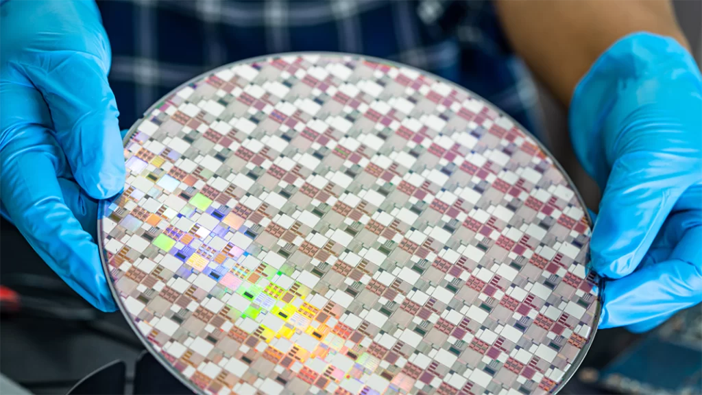
The work is done. Your devices are built. Now, the moment that can make or break everything – temporary bonding. One void, one misalignment, and yield is gone. The Apogee® Bonder delivers uniform, void-free bonds that hold through the final steps.
Home » Products » Bond / Debond » Apogee® Bonder
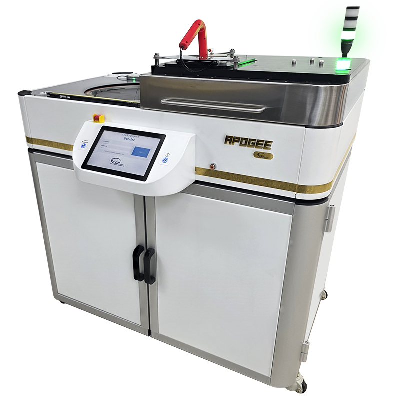
The work is done. Your devices are built. Now, the moment that can make or break everything – temporary bonding. One void, one misalignment, and yield is gone. The Apogee® Bonder delivers uniform, void-free bonds that hold through the final steps.
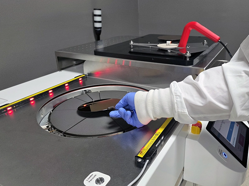
In-house bonding means no more delays, added costs, or limited control. Reduce turnaround time and per-wafer costs with the Apogee® Bonder. Don’t outsource your success to someone else.
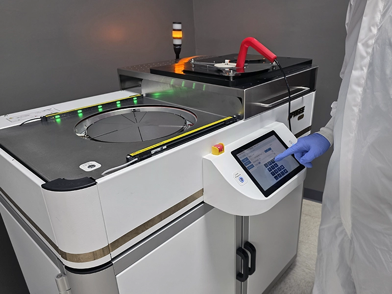
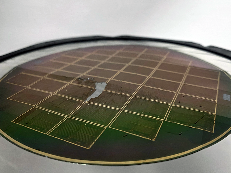
High Total Thickness Variation results in grinding errors, chipped edges, and lost yield in thinning and packaging – not to mention grinder contamination. Bonding under vacuum delivers uniform, void-free stacks: flat, stable, and ready for every step that follows.
Older equipment technologies require wafers to cool under bonding force. The Apogee® Bonder changes that. Dual heated platens stay at a constant temperature, producing uniform bonds in just minutes. Once done, the wafer pair safely cools off-line while the next cycle starts.
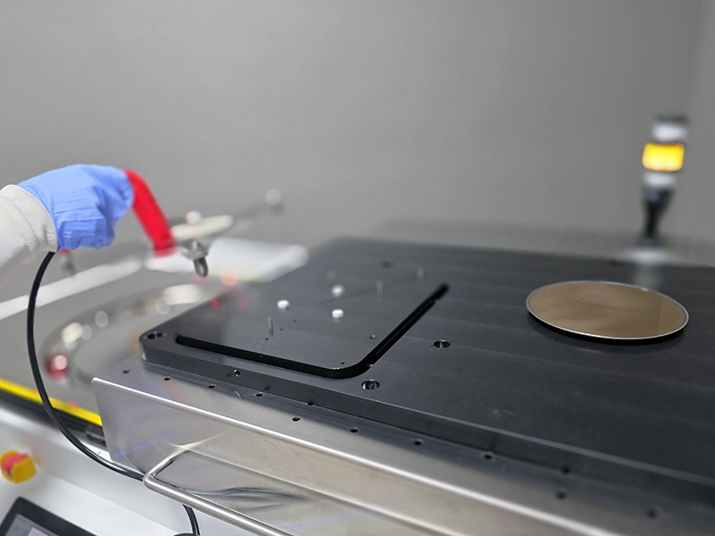
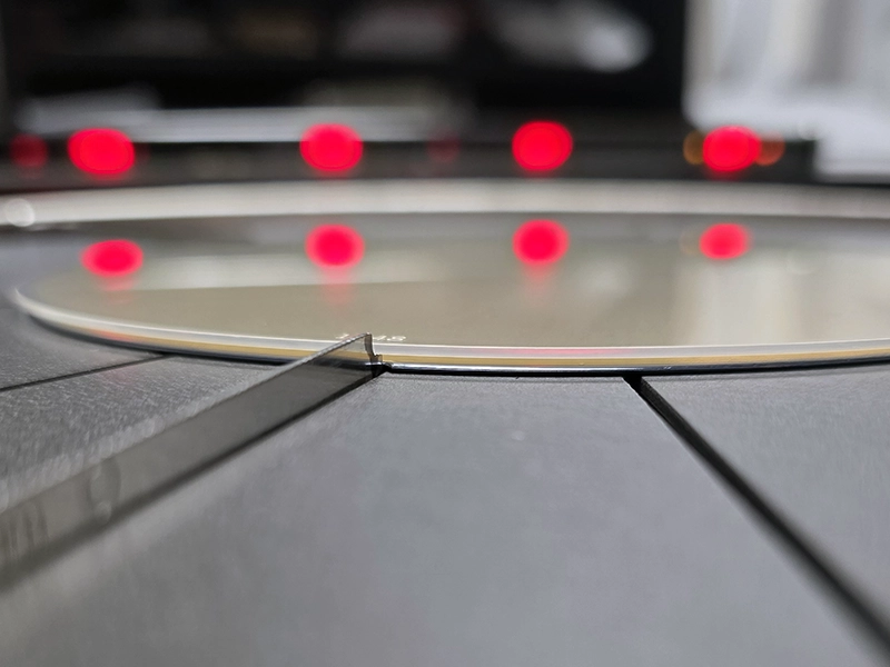
Track-like performance without the complexity or cost of robotic handling. The Apogee® Bonder provides reliability, repeatability, and tight process control you can count on for consistent results from lab to fab.

From R&D to production, the Apogee® Bonder adapts to your needs. Supporting wafers and substrates up to 300 mm, the platform grows and scales with you. Move from early development to full production with ease.
Engineered for superior performance, usability, versatility—and peace of mind.
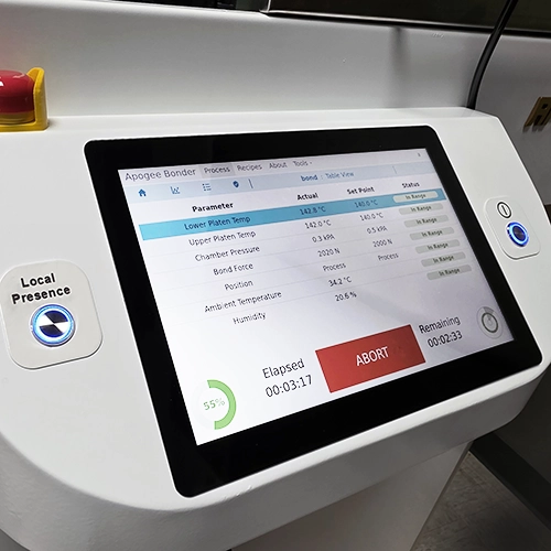
On-board 10-inch color touchscreen with DataStream™ OS included for visibility and your ease-of-use.
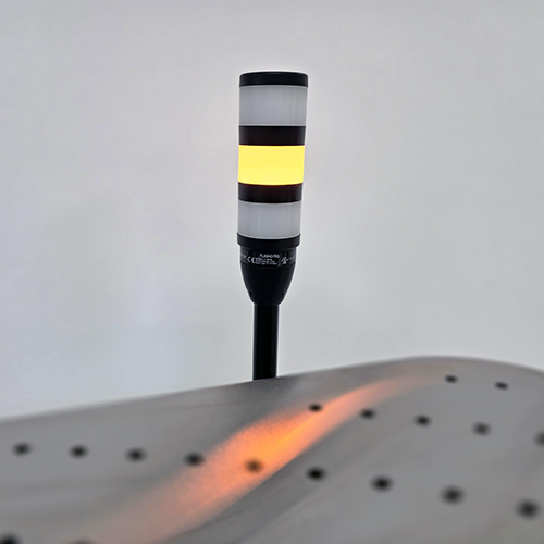
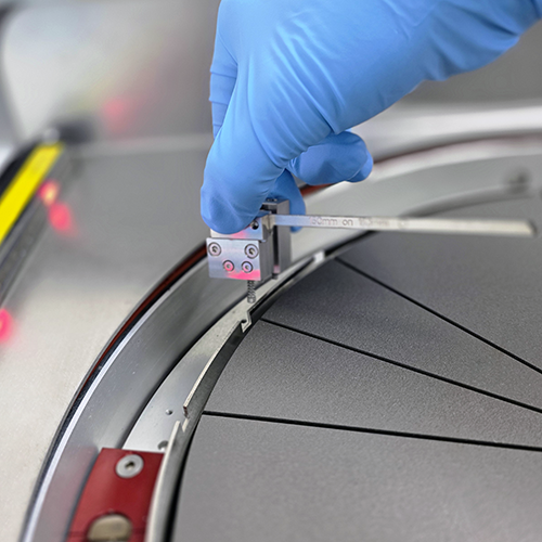
Interchangeable fixtures support rapid wafer diameter changes without tool reconfiguration, allowing multiple wafer sizes on a single platform.
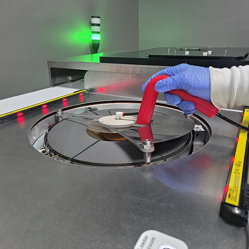
Vacuum transfer mechanism provides controlled wafer pickup and placement, ensuring consistent positioning and alignment during loading and unloading operations.
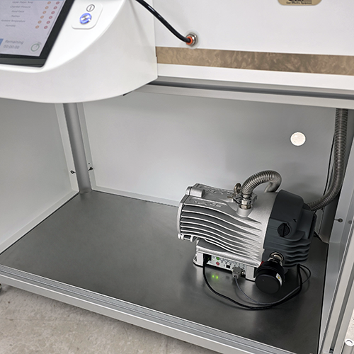
Supplies oil-free process vacuum to the bonding chamber, enabling cleanroom-suitable operation and stable process control, with integrated storage in the lower cabinet.
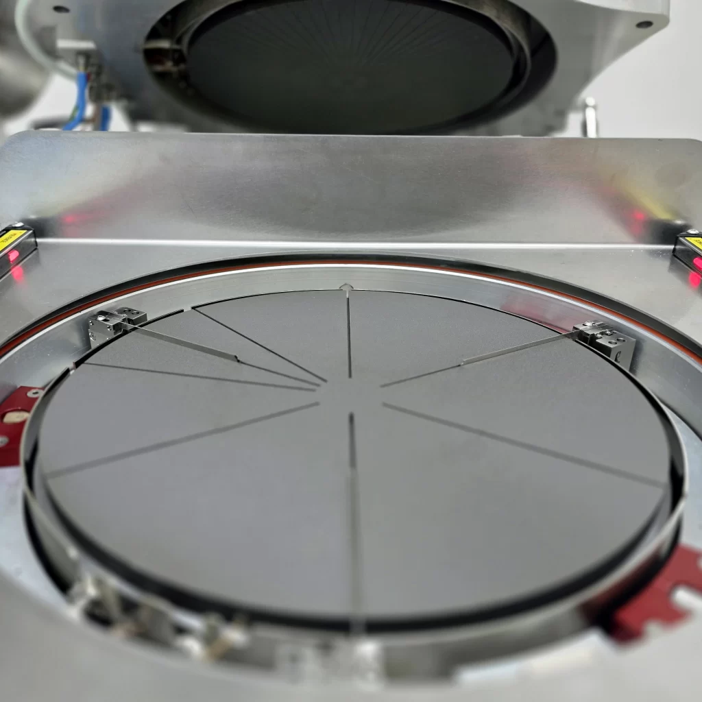
Independently temperature-controlled upper and lower platens enable uniform heating from both sides of the wafer, improving thermal consistency and supporting faster, more controlled bonding.
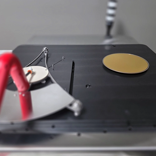
Provides a designated location for bonded wafer pairs to cool after processing, allowing the system to remain at temperature while the next wafers are processed.
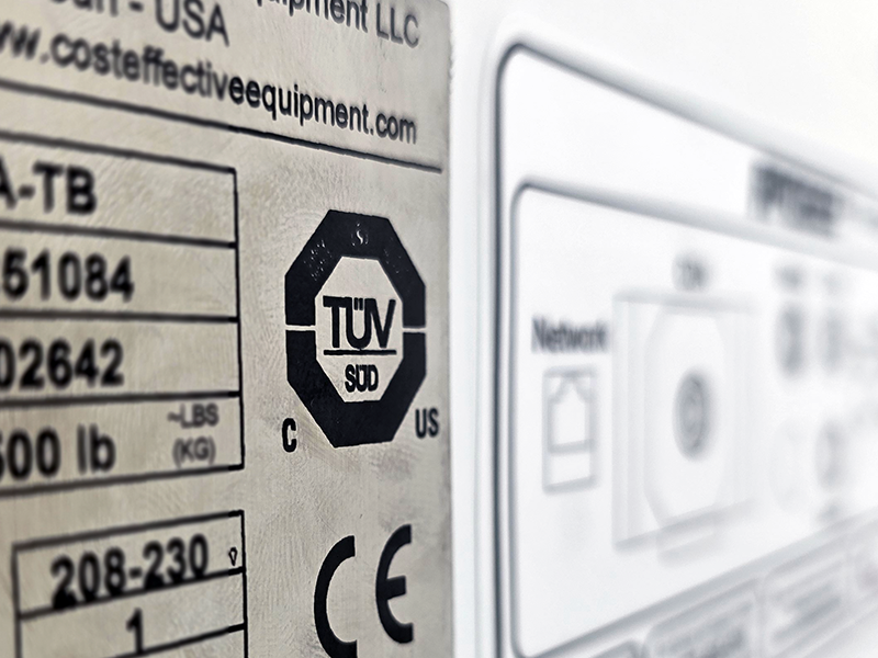
NRTL certification is crucial for semiconductor equipment, ensuring compliance with safety standards set by regulatory bodies like OSHA and ANSI.
Cee® bonders are NRTL listed right out of the box…
…your safety department is going to love you.
Knowledge is power. With DataStream™ technology, monitor and manage in real time, ensuring production-quality results from anywhere. Proactive warnings and detailed log files give you the information you need to succeed.
Process parameters and measurements are logged in real-time. Export in multiple formats for analysis, troubleshooting, and process optimization.
Access your Apogee® Bonder remotely via any web browser for real-time monitoring, adjustments, and recipe management. Create, modify, upload, download, and archive recipes seamlessly.
50 mm Round
300°C
550-12,000 N
300 mm Round
< 0.3% across working surface
10 N
<0.5 kPa (abs) in <90 sec
≤0.5 mm (dependent on substrate tolerances)
10″ Full Color Touchscreen (included)
Unlimited / Unlimited
0.1 s
500 lb (226.8kg)
1000 lb (453.6kg)
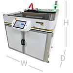
W: 48.5″ (1232mm)
D: 42.2″ (1072mm)
H: 52.8″ (1342mm)
W: 48″ (1220mm)
D: 75″ (1905mm)
H: 69″ (1753mm)
208-230 VAC
12.4A (max)
100-120 or 208-230 VAC
10A (max)
1/4″ Push to Connect, <20″ Hg (33kPa)
1/4″ Push to Connect, 50 psi (345kPa)
W: 13.25″ (337mm) W
D: 21″ (533mm) D
H: 13.25″ (337mm) H
With four decades of experience, our experts will collaborate closely with you to understand your requirements and deliver solutions that exceed expectations.
