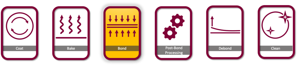
Wafer bonding is crucial for compact and powerful devices. It involves coating a full thickness wafer with adhesive, bonding it to a support carrier wafer, and thinning it for downstream processes. Key factors impacting bonding quality include flatness (TTV), alignment, voids, temperature control, CTE match, and bonding force. Addressing these factors ensures uniform bonding, precise processing, and high device yield, leading to reliable and high-quality semiconductor devices.
Wafer Bonding Overview
Over the past years, temporary substrate bonding gained popularity alongside the demand for smaller, more powerful devices. Thin substrates (<100µm) pose challenges in handling, but a temporary wafer bonder solves this, reducing breakage risks.
In the bonding process, a full thickness wafer with devices is coated with a temporary adhesive to withstand downstream stresses. It’s bonded to a support carrier wafer. After thinning and backside processing (e.g., TSV, metal-plating), the stack undergoes debonding, cleaning, dicing, and packaging.
Bonding Process Description
*This process description pertains to the Cee® Apogee® Bonder. While the processes of other manufacturers may vary slightly, the basic principles remain consistent throughout the industry.
After referring to the adhesive material manufacturer’s specifications, the bonder platens are heated to the temperature required for the bonding adhesive. This temperature is chosen based on the point that the material liquifies in order to maximize adhesion.
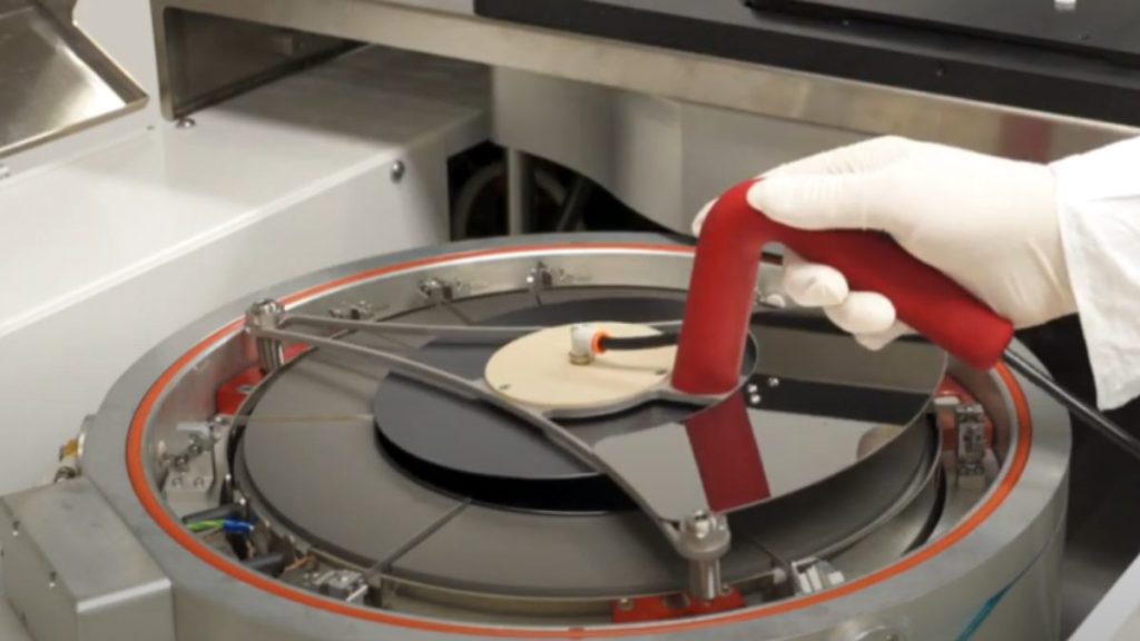
The device wafer is loaded onto the lower platen and centered using the built-in alignment fixtures. The carrier wafer is then placed and aligned on top of the device wafer. The mechanical alignment fixtures keep the carrier and device wafers separated at loading.
While the two wafers are held, the bonding chamber closes and vacuum is applied, evacuating air from the bonding chamber. Programmable piston force “squeezes” the wafers together for a specified period of time, planarizing the bonding adhesive and ensuring full wafer coverage.
Once complete, the chamber opens and the bonded wafer pair is removed and placed on a cooling plate. This allows the wafer stack to cool, setting the adhesive for maximum bond strength. The bonded wafer pair is then ready for the next downstream process step.
Bonding Factors
In the realm of wafer bonding, various critical factors profoundly impact quality. During the early days of Moore’s law, these parameters held less significance. However, with shrinking feature sizes and sub-100 micron thicknesses, and the growing number of devices per wafer, addressing these challenges has become crucial. Any alteration in these five parameters can significantly influence repeatability and throughput.
Flatness (TTV)
A high total thickness variation (TTV) can result in poor bonding uniformity, causing voids or incomplete bonding between the wafers. These voids can create weak spots in the bond interface, affecting the overall structural integrity and performance of the bonded device. Later, when the device is ground thin, non-uniformity, or in severe cases, grinding through the wafer can impact depth and conductivity leading to device yield loss and affecting the depth of focus for photolithography.
Alignment of Device Wafer to Carrier
The alignment of the device wafer to the carrier is of utmost importance in semiconductor manufacturing. It ensures uniform bonding, precise processing, and high device yield for downstream processes such as patterning, handling fixtures, and feature placement. Accurate alignment enhances overlay accuracy, eliminates edge issues, and optimizes throughput efficiency.
Voids
Voids in wafer bonding present significant challenges. They cause total thickness variation issues (see Flatness (TTV) above), impacting the uniformity of the bonded layers and potentially leading to breakage or de-lamination. Additionally, voids can trap and expand air during high-temperature processes or debonding, increasing the risk of structural damage or device failure. To ensure the integrity and reliability of the bonded wafers, avoiding voids is crucial, and precise control of the bonding process is essential to mitigate these problems effectively.
Temperature
Precise temperature control is crucial for successful wafer bonding. It ensures uniform adhesive reflow, preventing TTV and material distortions. With accurate control, adhesion issues are minimized, guaranteeing reliability and repeatability. By using dual platens for heating and carefully monitoring material bonding temperature, optimal results are achieved without compromising material integrity.
Coefficient of Thermal Expansion (CTE) Match
A good CTE match reduces stress and strain during temperature variations, preventing delamination and cracking in the bonded layers. This alignment guarantees the stability and reliability of the bonded structure, vital for the performance and longevity of the semiconductor devices. Without a proper CTE match, the wafer bonding may result in defects and compromised device functionality, making it a critical consideration to achieve high-quality and durable wafer bonds.
Bonding Force
Bonding force determines the strength and integrity of the bond between two wafers or substrates. Optimal bonding force ensures that the wafers are firmly and uniformly pressed together, leading to a robust and reliable bond interface. Low bonding force can result in weak bonding and delamination, while excessive force can damage the wafers or lead to undesirable stress in the bonded layers. Achieving the right bonding force is essential for high-quality semiconductor devices, as it directly impacts their performance, yield, and overall reliability.
The Cee® Apogee® Bonder
Tailored for semiconductor production, the Apogee® Bonder is ideal for permanent and temporary adhesive bonding and accommodates a wide range of debonding materials such as peel, thermal slide, laser lift-off, and chemical release. It prioritizes high yield and throughput without the expense and complexity of full automation. With precise bonding for wafer sizes from 50mm to 300mm and a weekly volume of 400-1,000 wafers, it ensures critical process control for downstream thinned wafer processing, achieving an impressive ≥98% yield.
The bonder’s onboard control panel offers a user-friendly browser interface for real-time status updates. It enables schedule creation, remote process parameter updates, tool usage monitoring, and access to complete process history, logs, and analytics—tracking piston pressure, force, temperature, vacuum, and cycle time. With offline backup, data analysis, and push notifications to web-enabled devices, you’ll always stay informed
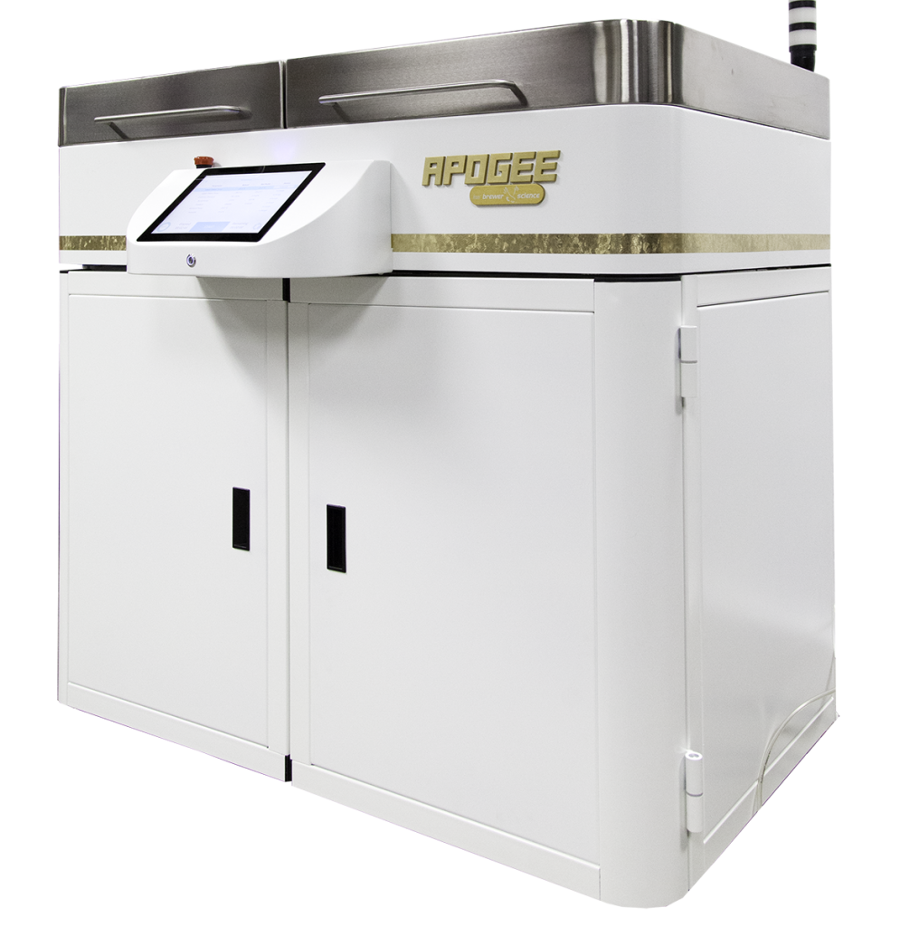
about the tool’s functionality and status, ensuring ultimate awareness of your process’ status anytime, anywhere.
The mechanical alignment fixtures are highly compatible with wafer notches and support the use of nonstandard wafers and carriers (alignment accuracy ≤ 0.5mm). Prior to bonding, the carrier and device wafer are separated, allowing for pre-bond evacuation and eliminating voids in the bond line. The dual ultra-flat (0.0005″ flatness specification), self-leveling heated platens with independent temperature controls ensure temperature uniformity of < 1% and bonding TTV as low as 5%. With a maximum bonding temperature of 300ºC and adjustable piston force (3.5 N – 12k N), accurate and precise bonds are guaranteed every time, with 10-N force resolution starting at 500 N.
Want to learn more? Contact our sales team today for more information!