
Beyond the Bond: Semiconductor Debonding Practices
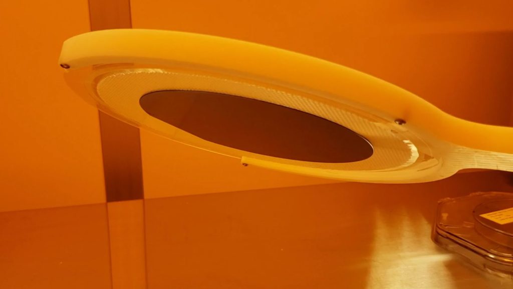
Debonding is a vital step in advanced semiconductor manufacturing and 3D Packaging that involves separation of the device wafer from its carrier. This article includes an overview of a variety of debonding methods, including Laser, Thermal, Chemical, and Mechanical Debonding along with crucial factors for success. The Vital Role of Debonding in Semiconductor Manufacturing Before […]