Edge bead removal is used to eliminate build up while backside rinse prevents contamination. Using an automated system for both processes results in precise, efficient, and consistent results with minimal operator intervention.
Introduction
Edge bead removal (EBR) and back-side rinse (BSR) are critical processes in the fabrication of high-quality micro and nanoscale devices such as sensors, solar cells, and microelectronics. In this post, we’ll dive deeper into edge bead removal and back-side rinse, outlining their use cases and traditional methods for achieving them.
Edge Bead Phenomenon
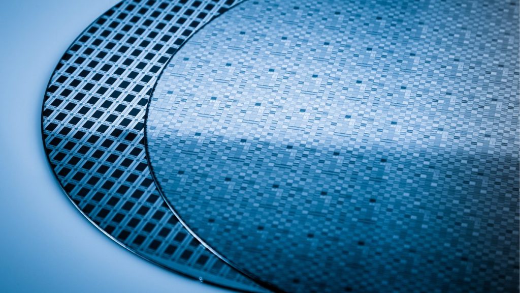
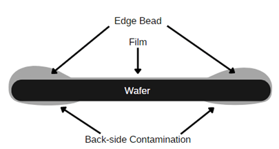
In spin coating, a liquid solution (such as a photoresist) is dispensed onto the center of a substrate. The substrate is then rotated rapidly, typically at speeds of several thousand rotations per minute, causing the liquid to spread outwards towards the edge of the substrate. This results in the formation of a thin, uniform film over the surface. During this process, the material tends to accumulate along the edges of the substrate, forming a ridge or bead.
Edge Bead Removal (EBR)
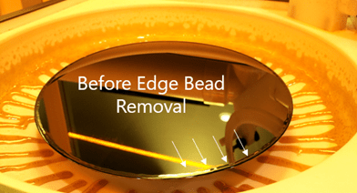
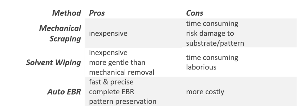
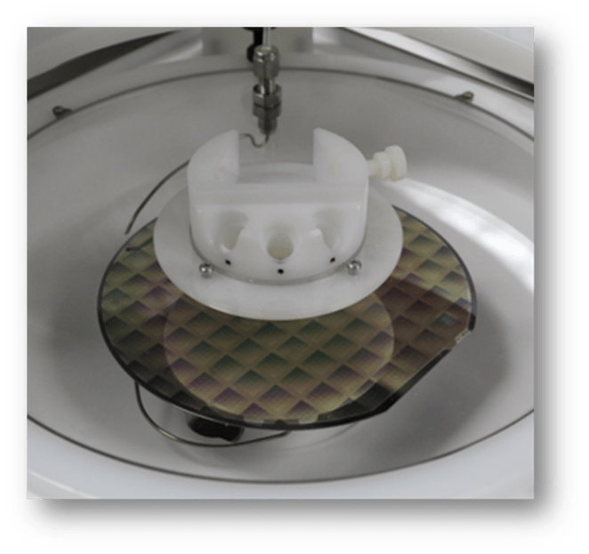
EBR is a process that removes excess material from the edge of a coated substrate preventing defects that may arise due to non-uniformity. Traditionally, there are three methods for edge bead removal. These are mechanical scraping, solvent wiping, and the use of a specialized automated edge bead removal system. Mechanical scraping (e.g., razor blade) is a simple and inexpensive method but causes damage to substrates and may compromise the photoresist pattern. Solvent wiping is far more gentle than mechanical scraping but requires time and effort to achieve full removal of edge bead. This is especially true when working with materials that do not dissolve easily. Automated edge bead removal systems are designed to selectively remove the edge bead without affecting the rest of the photoresist pattern as the spin process completes.
Back Side Contamination
During the spin coating process, material is dispensed. As the substrate spins, this material may migrate or splash onto the back of the substrate. If the back side of the substrate is not rinsed properly the contaminants and residues on the back side may contaminate the substrate and equipment in subsequent processing.
Back Side Rinse (BSR)
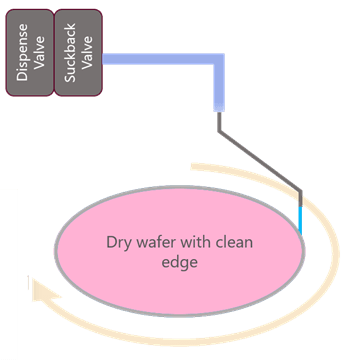
BSR is achieved by applying a rinse solution to the back of the substrate while it is spinning to remove residual photoresist or developing solution. The rinse is applied to the exposed underside of the substrate and is evenly distributed to the edge as the substrate spins. The result is a clean underside which is important for avoiding unwanted contamination and achieving precise and reliable results.
Conclusion
In summary, edge bead removal (EBR) and back side rinse (BSR) are critical processes in the fabrication of high-quality semiconductor devices. While methods vary, integrated automated systems for both EBR and BSR provide precise, efficient, and consistent results with minimal operator intervention. If you’re interested in learning more about our offerings, please contact our sales team today.