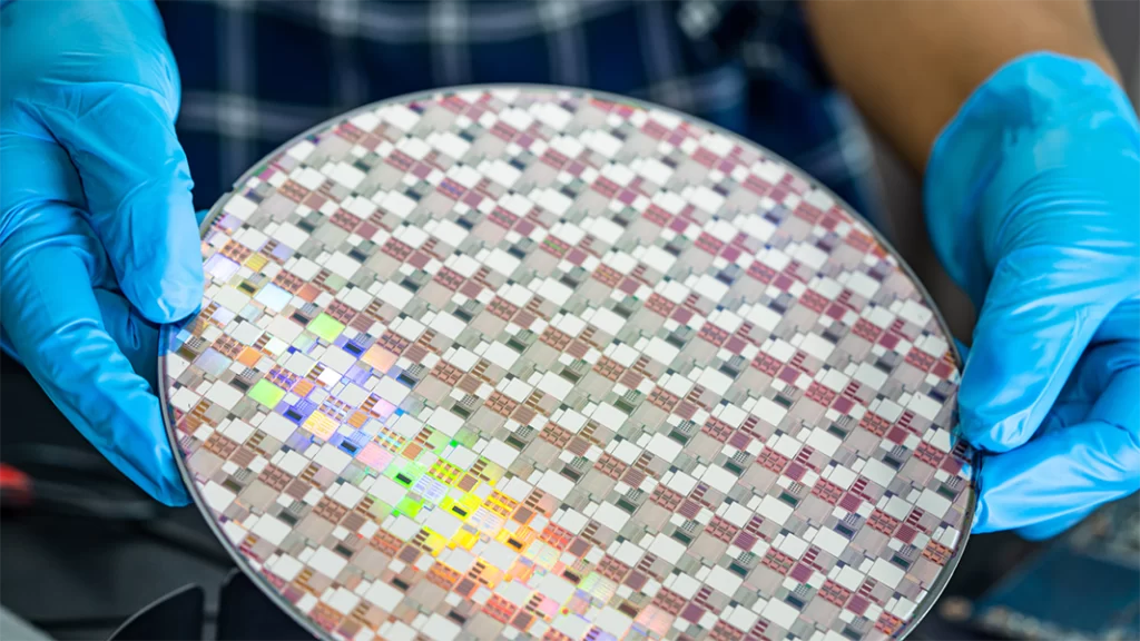
Temporary bonding is essential in modern semiconductor manufacturing, especially as devices have become thinner, more complex, and more fragile. This process is used to protect and support wafers during critical steps like thinning, backside processing, and advanced packaging.
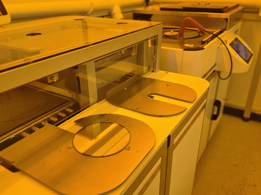
A device wafer is temporarily attached to a carrier wafer using a removable adhesive. The bonded pair allows the device wafer to be thinned and processed safely without damaging, warping, or breaking. After processing is complete, the wafers are separated, or “debonded”, using thermal or mechanical methods depending on the adhesive and process requirements.
Temporary bonding ensures high yields, safe handling, and access to advanced packaging techniques that would otherwise be too risky or impossible.
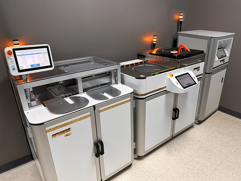
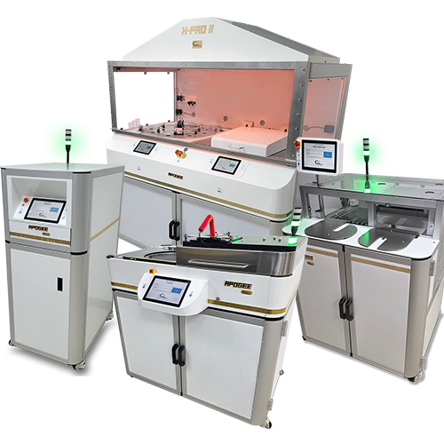
Advanced processes require advanced technology. Cee® equipment is tailored for lab-scale development and production, supporting a wide range of substrates and adhesive types.
Whether you’re new to temporary bonding or have it all figured out, Cee® supports every step. From adhesive selection to substrate compatibility and best-known methods, implement your process with confidence from day one.
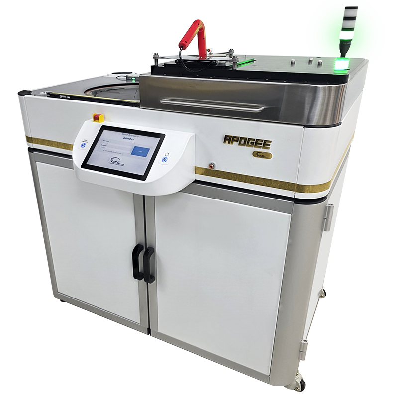
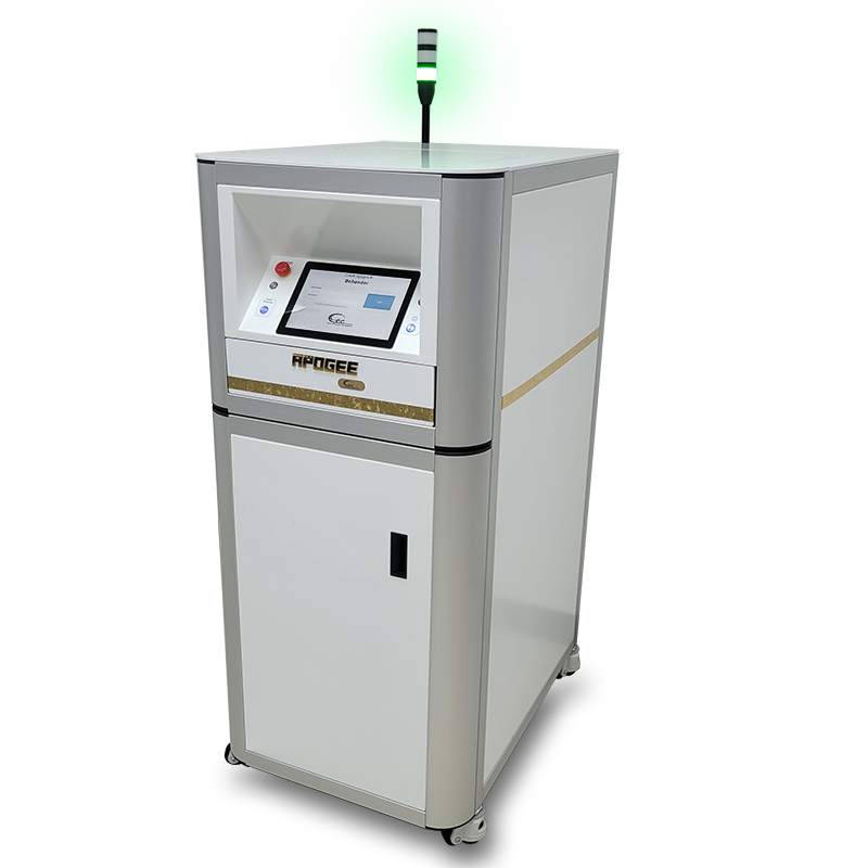
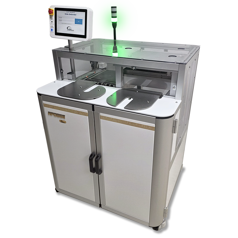
Premium Experience
Engineered for superior performance, usability, versatility—and peace of mind.
Intuitive Experience
On-board 10-inch color touchscreen with DataStream™ OS included for visibility and your ease-of-use.
Flexible & Scalable
Enables operation across multiple wafer sizes with configuration flexibility for immediate changes and future scaling.
User Friendly
Designed for ergonomic operation with layout optimized for efficient process flow and ease of use.
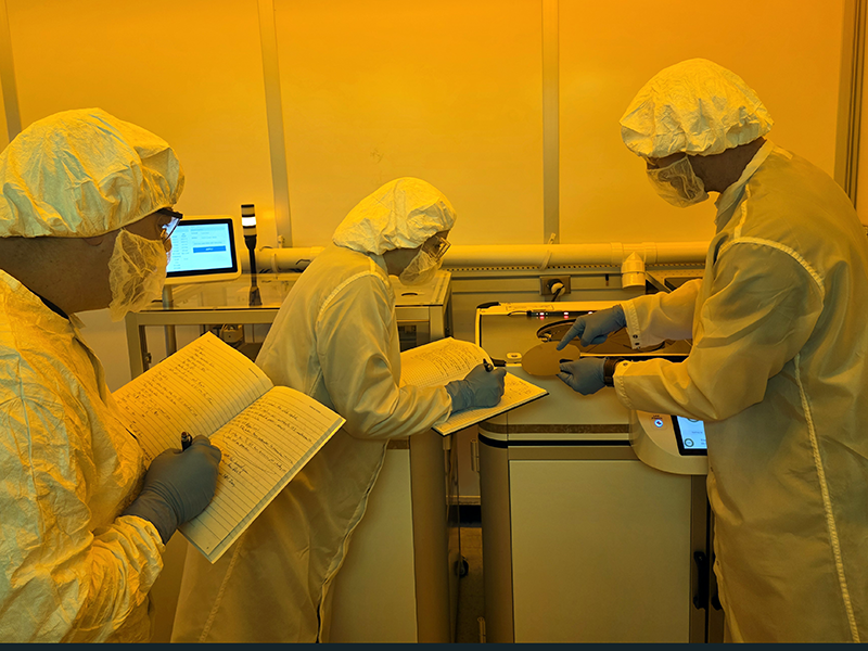
Lifetime Process Support
Process support available throughout the equipment lifetime to support long-term operation and evolving applications.
Easy Maintenance
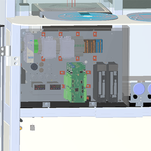
Designed for straightforward access to serviceable components, supporting efficient maintenance and reduced downtime.
Complete Family Suite
Simplify your equipment sourcing and receive expertise across all stages of adhesive coating, baking, bonding, debonding, and cleaning.
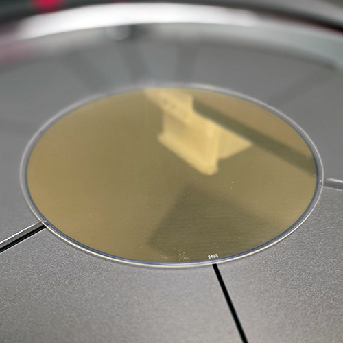
Thin, Brittle, Exotic
Yes, That Too...
Got GaAs? …or GaN, InP, sapphire, SiC diamond, metal foils, glass, silicon, or something else? Cee® bonding and debonding solutions handle the thin, fragile, weird stuff no one wants to break (and we make it look easy).
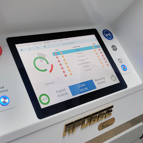
DataStream™ OS
- Included on every Apogee® Bonder and Debonder
Knowledge is power. With DataStream™ technology, monitor and manage in real time, ensuring production-quality results from anywhere. Proactive warnings and detailed log files give you the information you need to succeed.
Create and store unlimited recipes with unlimited steps. Use pre-defined commands to streamline your setup and execution.
Record Everything
Process parameters and measurements are logged in real-time. Export in multiple formats for analysis, troubleshooting, and process optimization.
Remote Access and Managment
Access your Apogee® equipment remotely via any web browser for real-time monitoring, adjustments, and recipe management. Create, modify, upload, download, and archive recipes seamlessly.
Monitor All the Things
DataStream™ technology monitors key parameters to ensure precise control for optimal results.
Safety
Leading the Charge
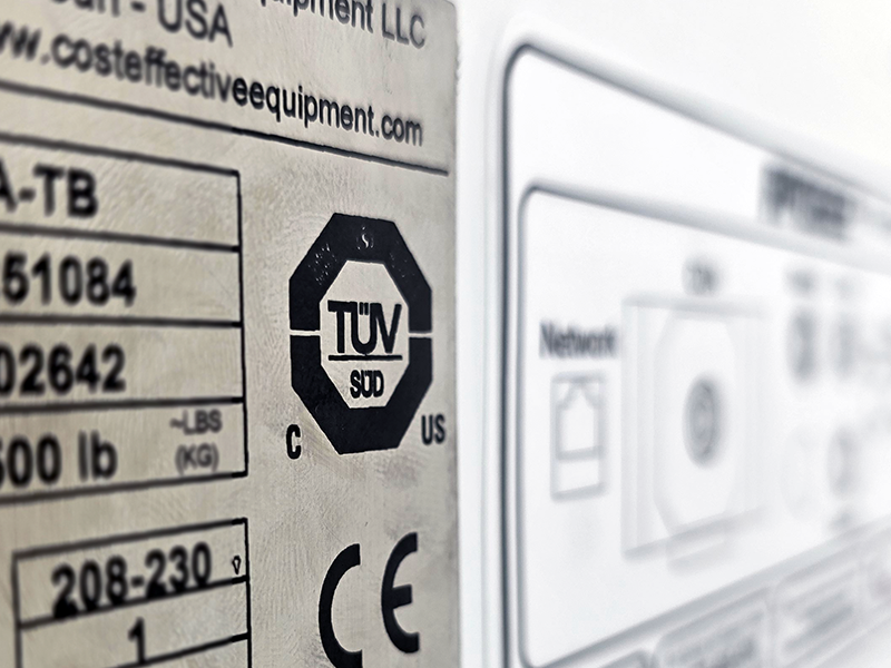
NRTL certification is crucial for semiconductor equipment, ensuring compliance with safety standards set by regulatory bodies like OSHA and ANSI.
Cee® Bonders and Debonders are NRTL listed right out of the box…