Thinner and delicate substrates are commonly used in the semiconductor industry, and their safe handling requires special techniques and spin chucks. These substrates can be made of various materials, including silicon, metal foils, and flexible polymer films, and are highly sensitive to mechanical and thermal shock.
Thin Wafer Processing Trends
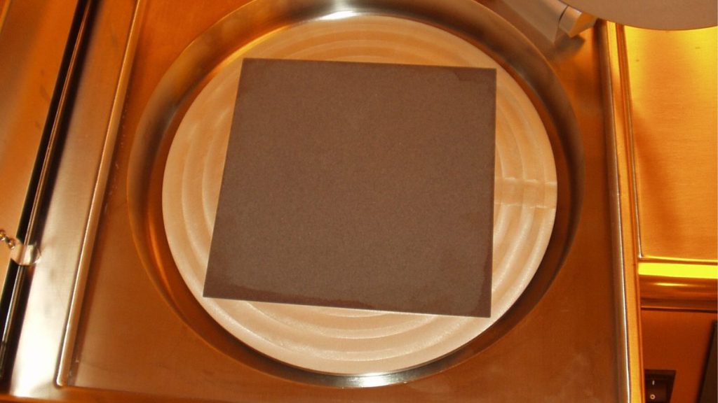
Thin and fragile substrates are now common throughout the semiconductor industry. Thicknesses of the substrates often range from 50 to 100 µm (0.001 to 0.004 inch) and are cut into various shapes (round, square, and rectangular). Safely handling these fragile materials requires specially designed spin chucks and thin-wafer handling techniques.
Thinned substrates can be made of a wide variety of materials such as flexible polymer films (fluorinated ethylene propylene [FEP] and polyester [PET]) and metal foils (titanium, aluminum, and steel). Other substrate materials include silicon, gallium arsenide (GaAs), gallium nitride (GaN), indium phosphide (InP), and silicon carbide (SiC). These CS and III-V materials are extremely brittle and far more sensitive to both mechanical and thermal shock.
Alternative Spin Chuck Designs
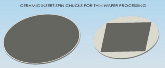
For thinned substrates (< 250 µm thick), we have developed a porous ceramic insert design that has a distinct advantage of completely supporting the backside of any given substrate dimension. The chuck distributes the vacuum equally through a porous surface
and mitigates any potential deflection, eliminating detrimental effects to your substrate or coat quality. These chucks are design specific and available for a wide array of shapes and sizes.
Film frames are commonly used to support silicon (Si) and CS materials. A device wafer can be mounted onto a film frame after backside processing but while it is still supported by its carrier, as recommended in the mechanical debonding process, or following separation (debonding) from the carrier, as in the thermal slide debonding process, for subsequent transport, cleaning, and packaging.
The porous ceramic design can also be adapted for thinned substrates mounted to film frames. Mechanical clamps and a porous ceramic insert combine for spin processing thinned substrates (< 250 µm thick) that have been taped to frames. The ceramic insert ensures complete and uniform backside support, while it distributes the vacuum source across the taped surface.
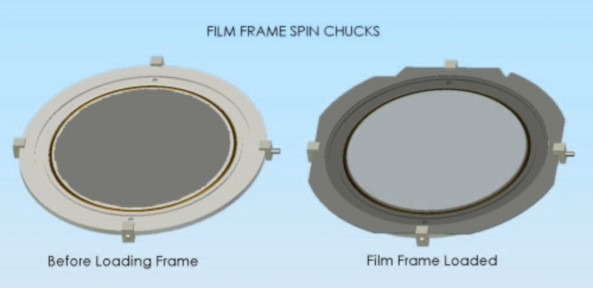
This design also utilizes vacuum O-rings and mechanical clamps for securing the outer film frame to the chuck assembly and maintaining positive lock.
Ready to take your thinned substrates to the next level? Our sales team is standing by to show you how our products and services can help you get there. Contact us today to learn more!