Beyond the Bond: Semiconductor Debonding Practices
Debonding is a vital step in advanced semiconductor manufacturing and 3D Packaging that involves separation of the device wafer from its carrier. This article includes an overview of a variety of debonding methods, including Laser, Thermal, Chemical, and Mechanical Debonding along with crucial factors for success. The Vital Role of Debonding in Semiconductor Manufacturing Before […]
Bonding and Debonding Indium Phosphide Wafers
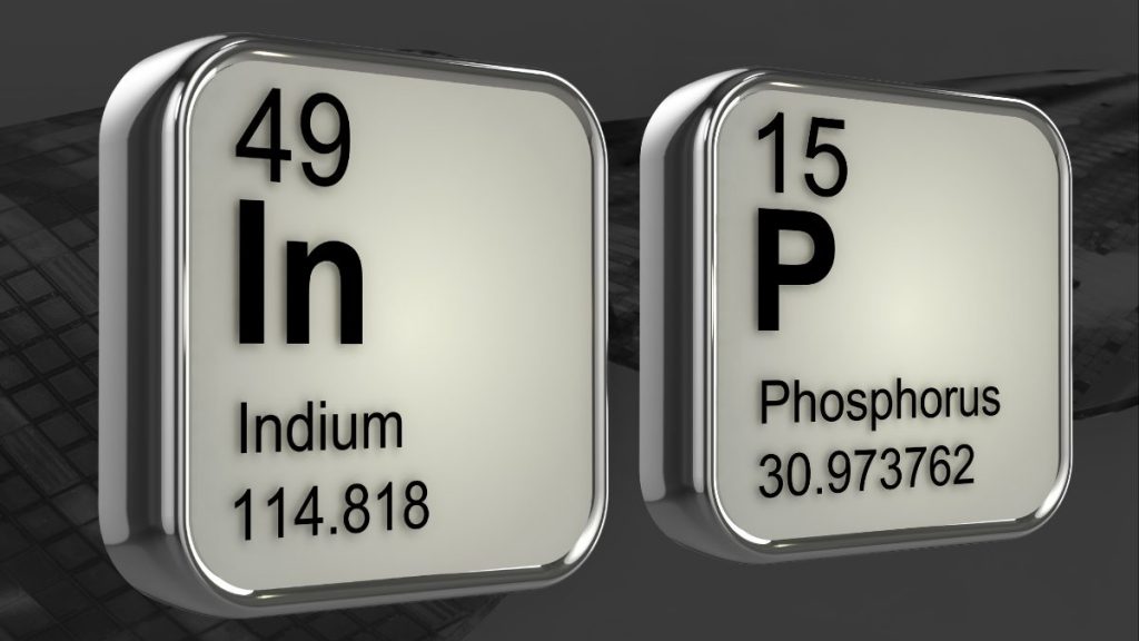
Indium phosphide (InP) wafers present challenges in bonding/debonding due to thermal mismatch, surface damage risks, and material compatibility issues. Cee® provides precision wafer handling tools with customized process controls designed to tackle the challenges presented by InP wafers. Experience reliable wafer handling and fully utilize the exceptional properties of InP for advanced electronics/photonics. Introduction Indium […]
Wafer Bonding Theory
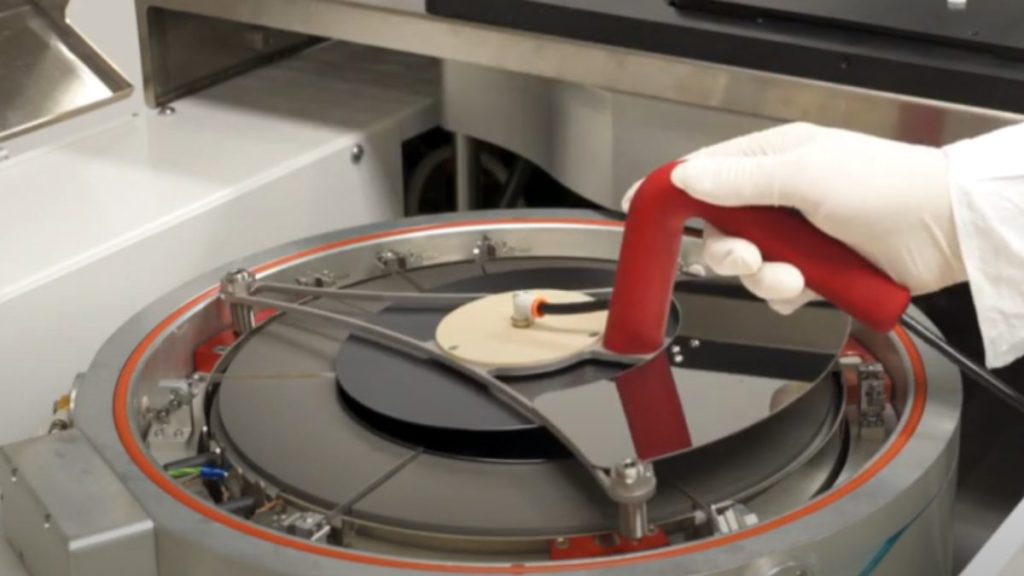
Wafer bonding is crucial for compact and powerful devices. It involves coating a full thickness wafer with adhesive, bonding it to a support carrier wafer, and thinning it for downstream processes. Key factors impacting bonding quality include flatness (TTV), alignment, voids, temperature control, CTE match, and bonding force. Addressing these factors ensures uniform bonding, precise […]